
Function
1. Providing materials characterization service fororganic/inorganic optoelectronic semiconductor and preparingtest report
2. Providing contract research and processdevelopment services in the field of optoelectronics and related areas.
3. Providing testing of optoelectronic devicesand equipment for the fabrication of optoelectronic devices
4. Providing consultancy and training services inthe area of organic optoelectronics, vacuum technology and nanotechnology.
Development Target
To raise the level of management of the laboratory and strive for public acknowledgement of its testing ability and to make it as a public testing organization with China Metrology Accreditation(CMA) and China National Accreditation Service for Conformity Assessment (CNAS).
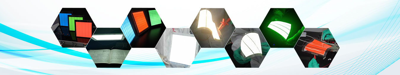
Prospective ServicesAreas
Microscopic techniques: scanning electronmicroscope, high-resolution optical microscope, etc.
Opticaland physical properties of materials: atomicforce microscope, UV-Vis spectroscopy, photoluminescence spectroscopy, ellipsometry,surfaceprofiler, etc.
Device properties: current-voltage-luminancecharacteristics, color characteristics, probe station for measuring electricalproperties of semiconductors, lifetime tester, etc.
Device processing: thermal evaporation, atomiclayer deposition, magnetron sputtering, plasma-enhanced chemical vapordeposition, glove boxes, glass scrubbers and ultrasonic cleaners, laserlithography, glass scriber, plasma treatment, UV-ozone treatment, materials synthesisfacilities, etc.